Reaction-Time Flappy Bird Game (Embedded Systems)
Real-time Flappy Bird-style game implemented on Terasic DE10-Standard SoC FPGA board, demonstrating embedded hardware/software co-design with C, Verilog, and AXI-Lite communication.
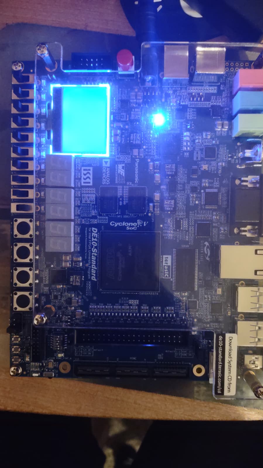
The Terasic DE10-Standard board with the game running on its LCD.
Demo video: a walkthrough of the code, then the game running on the board.
Project Overview
🎮 Embedded Gaming System
This project implements a reaction-based "Flappy Bird"–style game on the Terasic DE10-Standard SoC FPGA board, demonstrating embedded hardware/software co-design. The game challenges players to control a bird navigating through dynamically generated obstacles using physical push buttons, switches, and real-time visual feedback.
The system showcases the integration of real-time embedded software, digital logic design, and system-on-chip architecture, serving as a capstone example of embedded co-design principles.
🎯 Key Features
-
Hardware/Software Co-Design: HPS executes game logic while FPGA manages low-level I/O operations
-
Real-Time Performance: 60 Hz gameplay loop with consistent frame rate and deterministic timing
-
Multi-Domain Communication: AXI-Lite register interface enables seamless HPS↔FPGA synchronization
-
Hardware Input Processing: Debounced inputs, LED indicators, and 7-segment display updates
-
Visual Feedback System: 128×64 SPI LCD display with PWM-based backlight control
-
Collision Detection: Real-time physics with scoring and adjustable difficulty via board switches
🏗️ Technical Architecture
🔧 Hardware Platform
- Terasic DE10-Standard: Intel Cyclone V SoC FPGA with dual-core ARM Cortex-A9 HPS
- Display: 128×64 SPI LCD for game rendering
- Input/Output: Push buttons, slide switches, user LEDs, 7-segment display
💻 Software Stack
- HPS Domain: C programming for game logic, physics, and rendering loop
- FPGA Domain: Verilog for low-level I/O management and register interface
- Development Tools: Quartus Prime, Platform Designer (Qsys), GCC toolchain
🔄 System Architecture
HPS (C) ←→ AXI-Lite Bridge ←→ FPGA (Verilog)
    ↓                              ↓
Game Logic & Physics          I/O Management
Rendering Loop (60Hz)         Input Debouncing
SPI LCD Output               LED Control
                           7-Segment Display
                           PWM Backlight
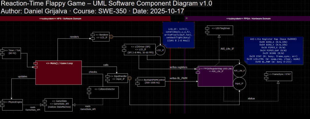
System component diagram
📡 Communication Protocol
- Shared Registers: Synchronized game states between HPS and FPGA domains
- AXI-Lite Interface: Low-latency communication for real-time control
- SPI Communication: High-speed LCD frame buffer updates
🎮 Game Implementation
🎯 Core Gameplay
- Reaction-Based Control: Player uses push buttons to control bird movement
- Dynamic Obstacles: Procedurally generated pipes with adjustable difficulty
- Real-Time Physics: Collision detection and scoring system
- Visual Feedback: LED indicators and 7-segment display for game state
⚡ Performance Optimization
- Hardware-Timed Loop: Consistent 60 Hz frame rate with deterministic timing
- Efficient Rendering: Optimized SPI communication for smooth graphics
- Low-Latency Input: Hardware-based input debouncing for responsive controls
🧪 Testing & Validation
- Structured Test Plan: Comprehensive validation of HPS↔FPGA communication
- Frame Integrity Testing: Verification of SPI rendering and display output
- Collision Logic Testing: Systematic validation of game physics
- System Responsiveness: Performance testing under various load conditions
🎯 Impact & Outcomes
✅ Technical Achievements
- Successful Integration: Seamless HPS and FPGA domain communication via AXI-Lite
- Real-Time Performance: Achieved consistent 60 Hz gameplay with hardware timing
- Hardware Optimization: Efficient I/O management with debounced inputs and PWM control
- System Reliability: Robust error handling and deterministic timing across domains
🌟 Key Learning Outcomes
- FPGA Development: Digital logic design and Verilog programming for embedded systems
- HPS Interfacing: ARM Cortex-A9 programming and system integration
- AXI Bridge Communication: Low-level hardware communication protocols
- Embedded Co-Design: Integration of software and hardware domains in SoC architecture
- Real-Time Systems: Deterministic timing and performance optimization for embedded applications
🔧 Technical Skills Demonstrated
- Hardware Description Languages: Verilog for FPGA logic implementation
- Embedded C Programming: Real-time systems programming on ARM architecture
- System Integration: SoC design and inter-domain communication
- Hardware Debugging: Low-level system testing and validation methodologies
💡 Project Significance
This embedded systems project demonstrates mastery of hardware/software co-design principles, showcasing the integration of real-time embedded software with digital logic design. The Flappy Bird implementation serves as a comprehensive example of SoC architecture, AXI communication protocols, and embedded systems development, highlighting expertise in FPGA programming, HPS interfacing, and real-time system optimization.
Project Details
- Role
- Embedded Systems Developer
- Timeline
- January 2024 – March 2024
- Status
- In Development
- Technologies
- C (HPS)VerilogQuartus PrimePlatform Designer (Qsys)GCC ToolchainAXI-LiteSPI Communication